Semiconductor
Application in Semiconductor industry
Measurement of silicon wafer thickness in lapping machine
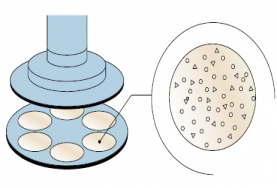
To lap the sliced silicon wafer to certain level of the surface roughness, gap sensors are mounted on the lapping machine with the accuracy of ± 3μm.
Measurement of wafer thickness
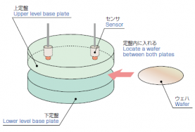
It measures the thickness of the silicon wafer prepared by slicing silicon ingot thinly.
The sensor detects the gap between the upper and lower level base plates to calculate the wafer thickness. 05 type sensors are mainly used, but also 09 type sensors are also occasionally used.
The sensor are embedded into the upper base plate.
Thickness measurement of Cu vapor deposition sheet
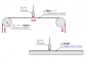
It measures thickness of Cu evaporated film by non-contact. The sensor can be used in vacuum chamber because of eminent environmental resistance.